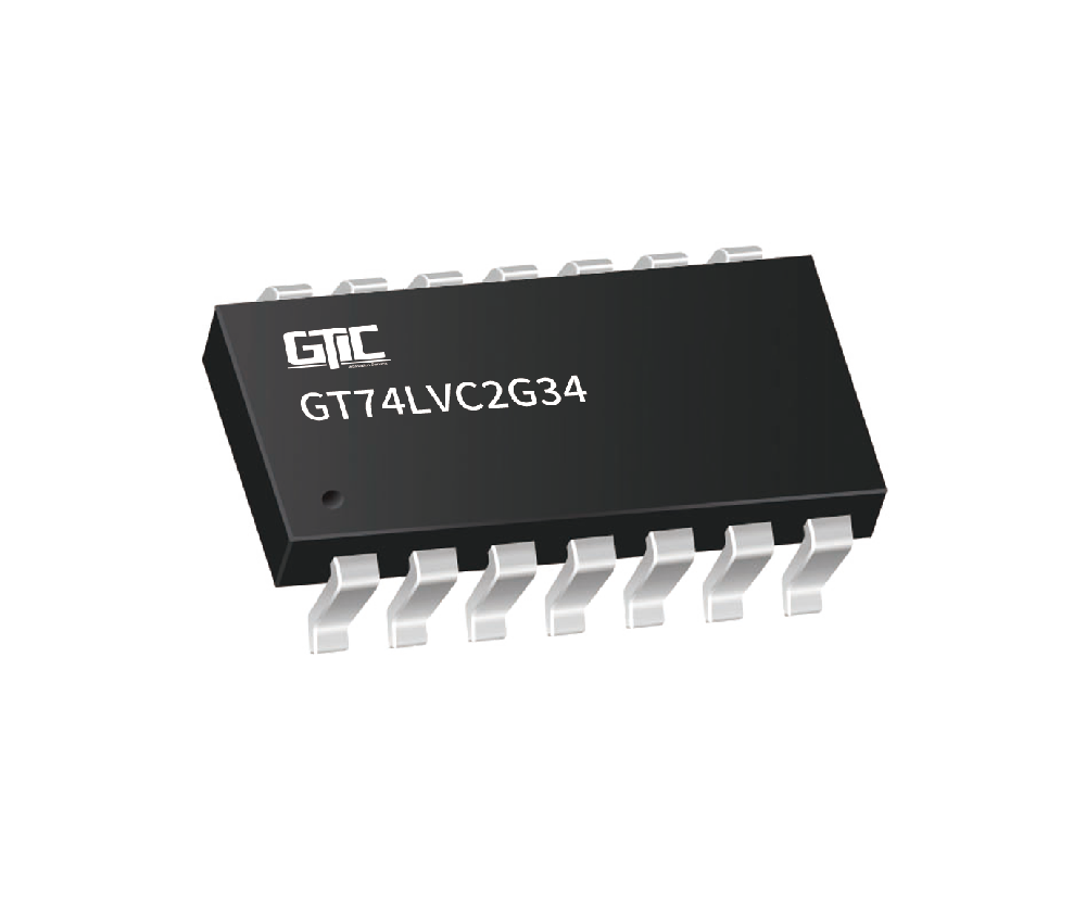


缓冲器
GT74LVC2G34
The operating voltage range of the dual buffer gate is 1.65 V to 5.5 V. The GT74LVC2G34 device contains dual buffer and performs the Boolean function Y=A. The CMOS device has high output drive while maintaining low static power dissipation over a broad VCC operating range. This device is fully specified for partial-power-down applications using Ioff. The Ioff circuitry disables the outputs, preventing damaging current backflow through the device when it is powered down.
特性
- Low Power Consumption, 10-μA Max ICC
- Supports 5 V VCC Operation
- Inputs Accept Voltages to 5.5 V
- Max tpd of 3.3 ns at 3.3 V
- ±24-mA Output Drive at 3.3 V
- Ioff Supports Partial-Power-Down Mode
- Typical VOHV > 2 V at VCC = 3.3 V, TA = 25°C
- Typical VOLP < 0.8 V at VCC = 3.3 V, TA = 25°C
应用
- AV Receivers
- Audio Docks: Portable
- Blu-ray Players and Home Theater
- Embedded PC
- MP3 Player/Recorder (Portable Audio)
- Personal Digital Assistant (PDA)
- Power: Telecom/Server AC/DC Supply
- Solid State Drive (SSD): Client and Enterprise
- TV: LCD/Digital and High-Definition (HDTV)
- Tablet: Enterprise - Video Analytics: Server
- Wireless Headset, Keyboard, and Mouse